A few years back, I upgraded my Christmas tree from a cheap string of warm white LEDs to a set of 100 WS2811 pixel LEDs driven by a Raspberry Pi. Naturally I chose Rust, and the original version can be found on GitHub. And while this has served me well, I felt that this year I needed my tree to be truly unique!
About 6 months ago, a co-worker was speaking about their experience with the Yosys opensource FPGA toolchain in their free time. Back at university, I had done a few modules on SystemVerilog and hardware design, using the excellent Cadence toolchain. So, I was curious to see how the opensource equivalent held up!
This led me to the decision to sink a lot more time than I should have into designing and implementing a custom processor, along with a custom ISA. Further, I decided to perform no research and just design and implement the entire design using only what I could remember. This meant taking no shortcuts and looking up existing Verilog designs for various components.
If you do not care about the specifics and just want to see the end result, then jump to the end of this blog post to see a video of the tree in action!
Hardware
My prior experience is with the Xilinx Spartan 3 range of FPGAs, however finding these either cheap enough or a model compatible with Yosys was not realistic. Instead, I decided to look into the Lattice iCE40 range of FPGAs, as they seemed to be in stock and relatively cheap on sites like eBay. The Lattice ECP5 range is much more capable but the price, on average selling for 3 times the amount, is not worthwhile for most small projects.
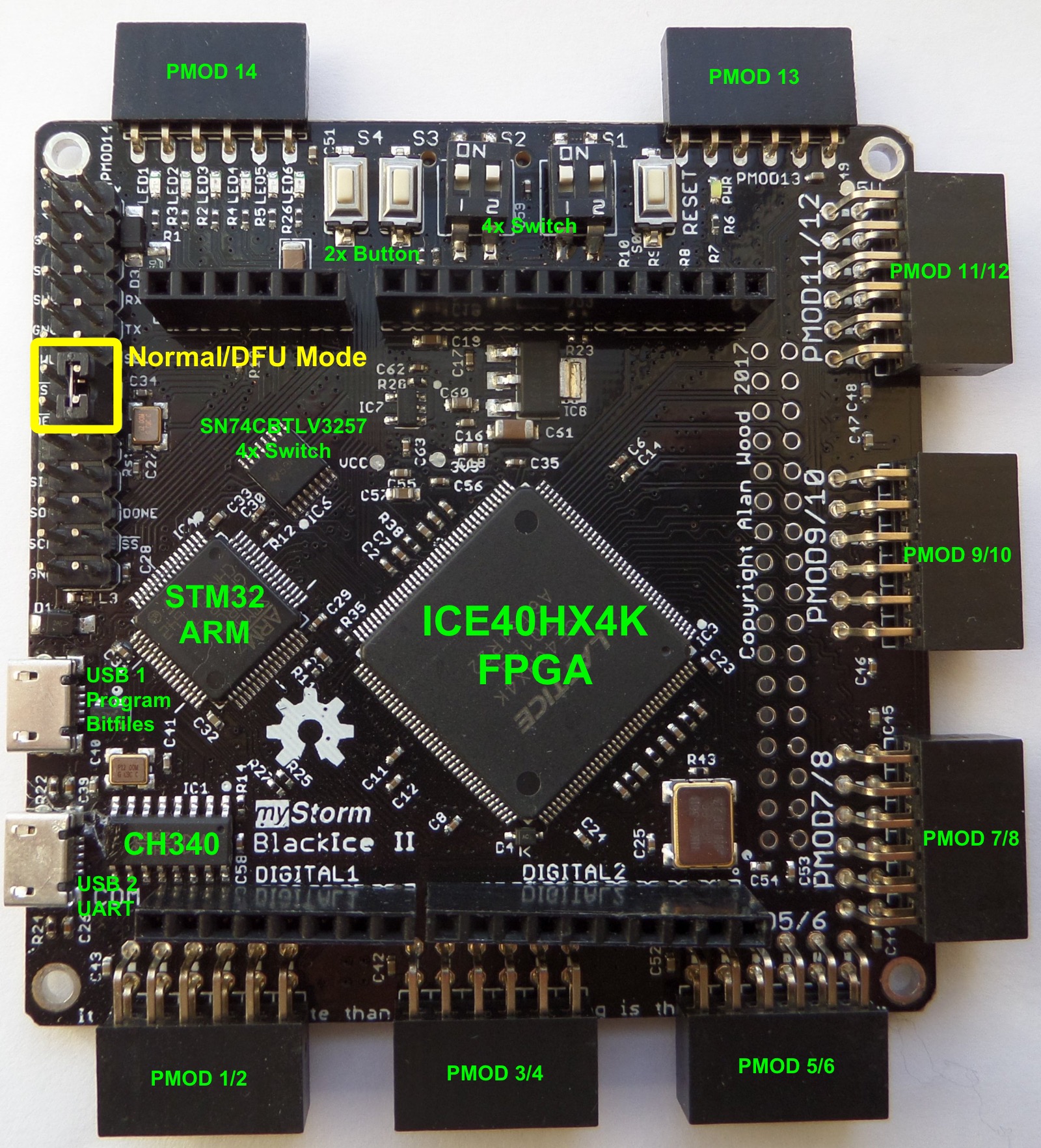 (Image source: https://github.com/mystorm-org/BlackIce-II)
I picked up a second hand BlackIce II development board for just under £40 on eBay and tried to load a simple flashing light bitpattern to the board. And… nothing! No matter what combination of power supply, USB cable or host I tried, I was unable to get any system to detect the board. I spent some time doing USB packet captures, and there seemed to be some issue occurring during the initial USB handshake. Weird!
At this point, I thought this project was dead in the water. However, after remembering there is a second USB port, which is intended for serial communication with your custom design running on the FPGA, I set out to design a custom firmware for the onboard ARM processor to get around the broken port.
The ARM processor is intended to bring up the FPGA on power up, and will not be used to implement any of the main functionality.
Custom firmware tangent
With the primary USB port out of action, I had to try and find a way of updating the firmware on the ARM chip. Luckily ARM processors implement a protocol called Serial Wire Debug (SWD) which is conceptually similar to the more well-known JTAG standard.
After patching the original firmware with support for uploading new bitstreams over the serial connection, flashing the firmware was as simple as connecting the SWD pins to a Raspberry Pi and using openocd to perform the upload. The main downside to this approach is speed and reliability. If I were going to develop the firmware further, I would look at getting a STlink to greatly speed up the process and remove the need for a Raspberry Pi.
A key issue with this custom firmware is that the serial port is now locked to the ARM processor and is no longer accessible from the FPGA. This is something I will have to work around in my system design.
The source code can be found here: blackice-ii-serialware.
System overview

When I started the project around 6 months ago, I decided to name the ISA Juna. I can’t exactly remember where that name came from, however it has stuck. Therefore, this initial processor design is called the J1 (Juna 1).
Key facts:
- The FPGA has a 100Mhz clock input, however this is divided down by a factor of 10x, due to overly deep and messy logic in my debug controller.
- The design features a debug controller, which is in charge of allowing external inspection and program uploads via the serial port. Due to the custom firmware hack, the ARM processor has to sit in the middle.
- The BlackIce II board features 512Kbit (256k x 16bits) of SRAM. The access time is quoted at 10ns and is the main limiting factors in the design. While it would be possible to speed up the design, there is little point without either implementing caching or using faster memory. The RAM controller is in charge of multiplexing access to the SRAM based on a priority order.
- The design is single core. I didn’t feel like my Christmas tree needed to be multicore. Maybe next year?
- There are 16x 32bit registers, with the last register storing the program counter. In hindsight, using 32bit registers was unnecessary!
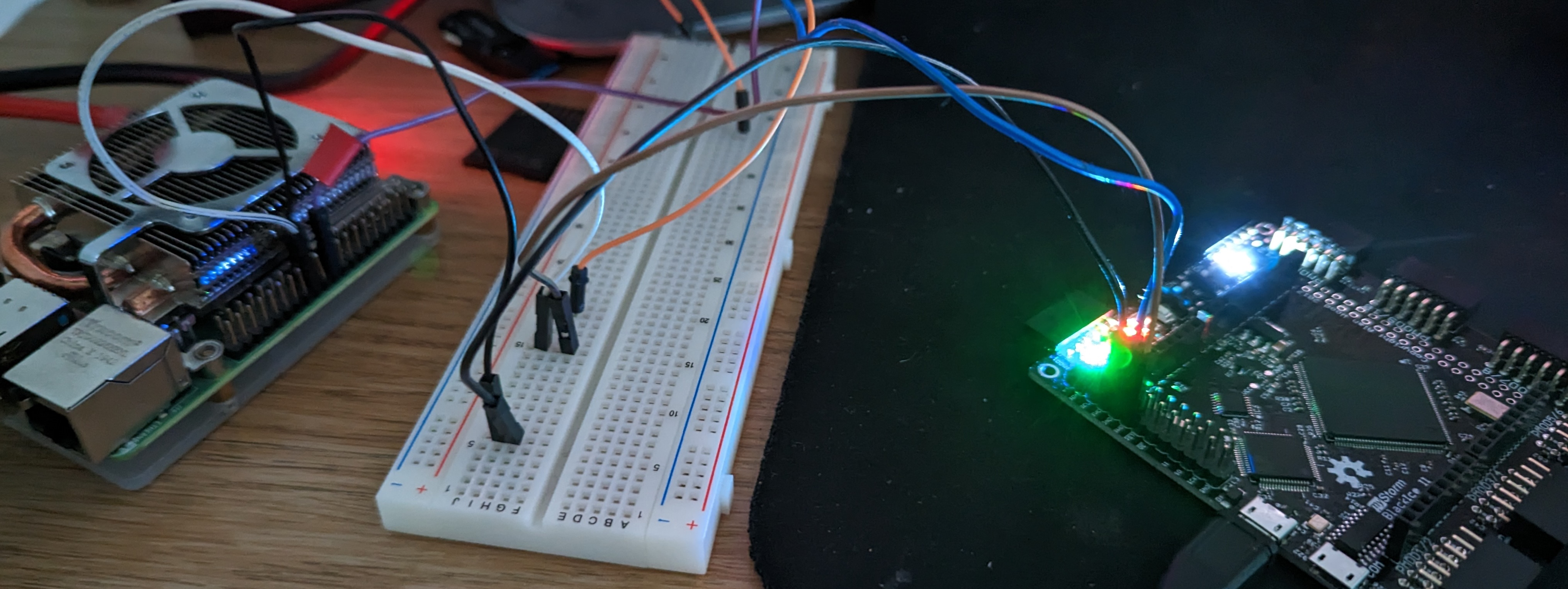
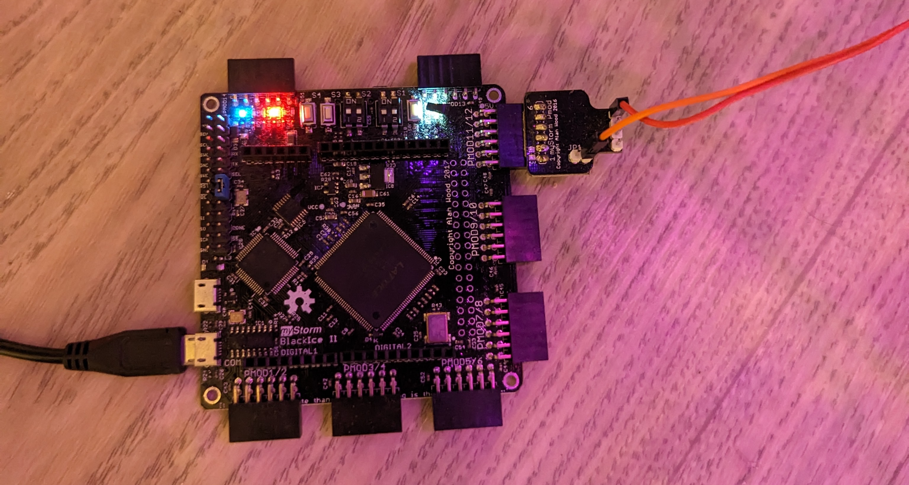
- The board features PMOD interfaces, which are a standardised connector and pin layout. I have connected my tree to one of these ports, via some dodgily soldered connectors.
- The WS2811 driver is in charge of ensuring the correct timings for driving the string of 100 WS2811 pixel LEDs connected to the board.
While I haven’t calculated properly or measured, earlier in the implementation phase I estimated the instructions per second to be around 2Mhz. Not a very impressive number when you consider modern processors, however my Christmas tree will just have to deal with it.
WS2811 driver
The WS2811 pixel LEDs use a single wire communication standard, which involves precise timings to signal the difference between a 1 and a 0. Each of the 100 pixels are individually controllable, however as they are connected in series, they must all be updated in one go. This therefore means the processor must produce a frame in memory and then have this flushed out to the pixels in one go.
In my design, the Juna core and the WS2811 driver are both wired directly into the RAM controller, allowing both of these components to interact with RAM. There is one caveat in that the SRAM is single port, meaning only a single address can be read or written at any given point in time.
Due to the precise timings required by the WS2811 lights, the WS2811 driver has the highest priority and any of its pending requests will be served before the Juna core. This means that from time to time, the Juna core will pause while it waits for memory access.
When the processor has produced a new frame, it sends over the address to the driver, which will automatically read the bytes from main memory and start outputting the data over the PMOD interface.
Juna core

The Juna processor is a simple non-pipelined in-order processor. I was originally planning on implementing a pipelined processor, however after some back of the napkin math, there seemed to be little to no point in this, due to the slow memory speed. I’m sure glad I choose to simplify the design, as this project would have taken much longer and been a lot harder to debug!
The diagram is an over simplification of the stages, however they are more or less what you would expect in a farily trivial old-fashioned processor.
Implementation
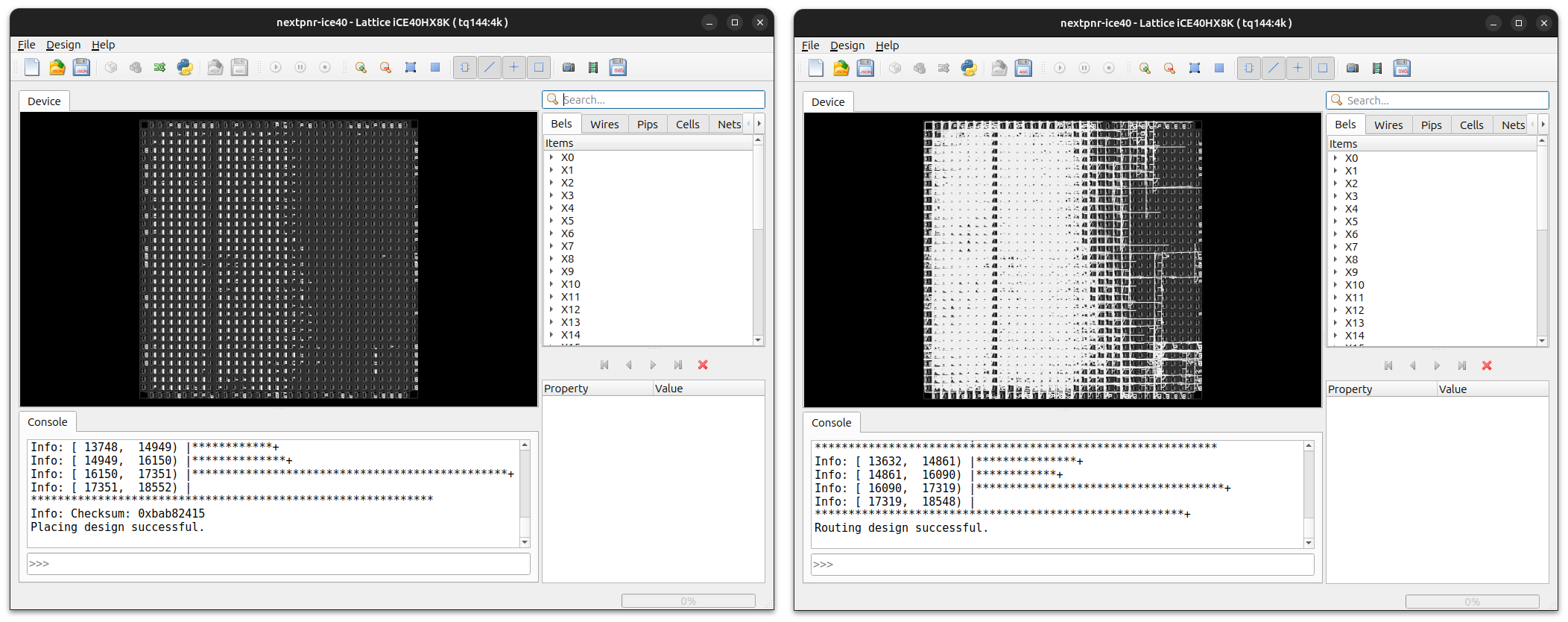
As alluded to earlier, this project is my first time using the Yosys toolchain. It is impressive what is available given that this is completely free! However, as can be expected, there are definitely a few rough edges, such as segfaults if you use a command incorrectly.
The above two images show the output of the Place and Route operations. The UIs are fairly minimal and for the most part, I automated away the need to use them via a Makefile:
build-chip:
	yosys -p "plugin -i systemverilog" -p "read_systemverilog blackice.sv" -p "flatten" -p "proc" -p "tribuf" -p "opt -full" -p "memory" -p "opt -full" -p "fsm" -p "opt -full" -p "synth_ice40 -top blackice -json chip.json"

build: build-chip
	nextpnr-ice40 --hx8k  --package tq144:4k --json chip.json --pcf blackice-ii.pcf --asc chip.asc --freq 25
	icepack chip.asc chip.bin

upload:
	./swtool upload /dev/ttyUSB0 chip.bin
In comparison to what I’m used to, there was a fair bit more trial and error required in order to get the toolchain configured.
assign bus_data = bus_addr == 3 ? value : 'z;
By default, tristate signals, such as those commonly used in buses, do not work. Even worse, there is no error! Instead
compiler will optimise away the logic and you’ll have some odd behaviour. After some Googling, I came across a post
saying that the tribuf pass needed to be enabled.
Yosys only includes support for Verilog by default, whereas I’m more used to SystemVerilog. There is a third-party module available called synlig which offers SystemVerilog support. One issue I came across after reinstalling my machine was that Yosys had a breaking update which caused synlig to no longer build. This was a bit of a pain to workaround, and if I hadn’t already used it, I would have likely given up!
The route stage takes a lot longer than I remember Cadence taking, however this may just be down to this being on a much smaller FPGA, therefore making the process more complex.
always @(posedge clk) begin
[...]
  case (state)
  [...]
  `STATE_EXEC1: begin
    priority casex (instruction[15:8])
      8'b0000_xxxx: begin : AND_INST  // ADD
        r_a_addr <= instruction[3:0];
        r_a_wdata <= reg_a + r_a_rdata;
        r_a_write <= 1;
        state <= `STATE_FETCH0;
      end
      8'b0001_xxxx: begin  // SUB
        r_a_addr <= instruction[3:0];
        r_a_wdata <= reg_a - r_a_rdata;
        r_a_write <= 1;
        state <= `STATE_FETCH0;
      end
      [...]
    endcase
    [...]
  end
  [...]
  endcase
[...]
end
Most of the Juna core’s implementation is your usual Verilog affair. On each clock cycle, I check the current state and input, and then assign the next state. In Verilog, you get a lot of goodies for free, such as not having to implement basic operations like addition from scratch! Anyone who has had to produce a adder from scratch by drawing out each individual wire in Cadence will tell you how tedious that process becomes!
The complete design, once place and routed looks fairly pretty. As I mentioned earlier, the iCE40 is more than capable for most hobby projects! As can be seen, there are still a lot of free cells left on this FPGA and if I could remove the overly complex and weird debug controller, then there would be even more space available.
The full Verilog source code can be found here: juna.
Instruction set
Now that I have covered the low-level details, it’s time to cover what actually runs on this processor.
Instructions are 16bits wide, which is the same size as the memory bus. As there are 16 registers, 4 bits are needed to encode each register. Registers 0-14 are general purpose, while 15 is reserved for the program counter (PC). User programs can access the PC register, such as to implement an unconditional jump.
Maths operations
| Name | 15-12 | 11-8 | 7-4 | 3-0 | Comment |
|---|---|---|---|---|---|
| ADD | 0000 | AAAA | BBBB | DDDD | D = A + B |
| SUB | 0001 | AAAA | BBBB | DDDD | D = A - B |
| XOR | 0010 | AAAA | BBBB | DDDD | D = A ^ B |
| XOR | 0011 | AAAA | BBBB | DDDD | D = A & B |
| ORR | 0100 | AAAA | BBBB | DDDD | D = A | B |
| SHF | 0101 | AAAA | BBBB | DDDD | D = A « B or D = A » B if B is neg |
Constants
| Name | 15-12 | 11-8 | 7-4 | 3-0 | Comment |
|---|---|---|---|---|---|
| LCB | 1010 | AAAA | BBBB | BBBB | D = literal(B) |
The LCB allows registers to be initialised to some constant literal. This instruction is very efficient as it does not
need to fetch from memory, however there is the limitation that it can only hold a byte.
Branching
| Name | 15-12 | 11-8 | 7-4 | 3-0 | Comment |
|---|---|---|---|---|---|
| BEQ | 1011 | AAAA | BBBB | DDDD | PC = D if A == B |
| BLT | 1100 | AAAA | BBBB | DDDD | PC = D if A < B |
| BLE | 1101 | AAAA | BBBB | DDDD | PC = D if A <= B |
| BLTS | 1110 | AAAA | BBBB | DDDD | PC = D if A < B (signed) |
Memory operations
| Name | 15-12 | 11-8 | 7-4 | 3-0 | Comment |
|---|---|---|---|---|---|
| LDB | 1111 | 0000 | BBBB | DDDD | B = byte at addr D |
| STB | 1111 | 0001 | BBBB | DDDD | byte at addr D = B |
| LDS | 1111 | 0010 | BBBB | DDDD | B = short at addr D |
| STS | 1111 | 0011 | BBBB | DDDD | short at addr D = B |
| LDW | 1111 | 0100 | BBBB | DDDD | B = int at addr D |
| STW | 1111 | 0101 | BBBB | DDDD | int at addr D = B |
If the address register (D) is the PC register (15), then a special case is triggered. After reading/writing to the
address stored in the PC register, which will be the space directly after the current instruction, the PC will also be
incremented by the size of the read, such as 4 bytes for LDW. This special case simplifies large constant loading, as
any arbitrary 32bit integer can now be encoded as a 6 byte instruction.
Port operations
| Name | 15-12 | 11-8 | 7-4 | 3-0 | Comment |
|---|---|---|---|---|---|
| TCP | 1111 | 0110 | BBBB | DDDD | Send B to device with addr D |
The port operations allow the Juna core to communicate with other hardware on the chip.
Currently only one device exists, which is the WS2811 controller with ID 1. Sending an address to that port will cause controller to read 300 bytes (RGB * 100) from that memory address and output them to the LEDs. It assumes RGBRGBRGBRGB… encoding.
The instruction set is fairly basic and places most of the hard work onto the user code. Where possible, if an operation can be implemented in user code, it is left for user code.
I came across this handy tool called customasm which allows you to describe your instruction set and let it handle assembling your code. This saved a lot of time! I was originally planning on implementing an assembler from scratch, however debugging both a processor and assembler at the same time did not sound like much fun.
#ruledef
{
    nop => asm { and r0, r0, r0 }
    mov {d: register}, {a: register} => asm { and {d}, {a}, {a} }
    add {d: register}, {a: register}, {b: register} => b @ d @ 0b0000 @ a
    sub {d: register}, {a: register}, {b: register} => b @ d @ 0b0001 @ a

    [...]

    pushw {r: register} => asm {
        lcb i1, 4
        sub sp, sp, i1
        stw {r}, sp
    }
    popw {r: register} => asm {
        ldw {r}, sp
        lcb i1, 4
        add sp, sp, i1
    }
As can be seen, you can describe pseudo instructions using other instructions. This means that, while the processor doesn’t have any instructions for pushing and popping from a stack, there is a pseudo instruction for this, greatly simplifying writing user code.
In my assembly language, I have reserved register 14 for the stack pointer (sp), and registers 12-13 for pseudo instructions use (i1, i2). Careful user code may still use i1 and i2, but it must be aware that the values may get overwritten.
The full set of instructions can be found here: juna.asm
Demo
After spending so much time implementing this custom processor, there wasn’t much time to implement surrounding tooling, such as a higher level language. Writing tree light patterns in assembly is a slow and error-prone. Therefore, I have only implemented a couple of patterns.
A small snippet of what a pattern looks like in assembly (not the pattern in the video):
fn_rainbow:
pushall
mov r11, r0
mov r6, r1

ldc r5, 255
ldc r7, hsl_table
ldc r8, 1
ldc r9, 0
ldc r10, 100

mov r2, r9
sub r2, r9, r8
sub r2, r2, r8

.loop:

; ensure in range
and r6, r6, r5

; r4=r6*3
mov r4, r6
add r4, r4, r6
add r4, r4, r6

; index into table
add r4, r4, r7

; r
ldb r0, r4
shf r0, r0, r2
stb r0, r11
add r11, r11, r8
add r4, r4, r8

; g
ldb r0, r4
shf r0, r0, r2
stb r0, r11
add r11, r11, r8
add r4, r4, r8

; b
ldb r0, r4
shf r0, r0, r2
stb r0, r11
add r11, r11, r8
add r4, r4, r8

; increment cycle pos
add r6, r6, r8

sub r10, r10, r8
beq .exit, r10, r9
brn .loop

.exit:
popall
ret
You may notice the use of hsl_table in the above assembly. If you recall the instruction set for this processor, there
aren’t any floating point operations, which makes performing interesting colour operations difficult.
hsl_table:
#d8 255, 0, 0
#d8 255, 6, 0
#d8 255, 12, 0
#d8 255, 18, 0
...
Therefore, I have cheated and embedded a lookup table for the exact special case I need.
Maybe next year I’ll return to this project and design a higher level language, which will allow me to more easily design and implement more interesting patterns, such as those the original Rust version had.
My main takeaway from this project is that Verilog and processor design is lot more approachable than you may realise. I strongly encourage you to consider giving it a go. Advent of code is popular on the software side, maybe we need a Advent of Verilog to get more people interested in hardware!